Wiring the Breadboard
First solder the header pins to the level shifter and GPS breakout boards. The easiest way to do this is to place the header pins in the breadboard, align the breakout boards with the pins, and solder each pin to the corresponding pad. For the GPS breakout board, only one side has header pins so you might have put something under the other side to make a stable base for soldering.
Note: Here’s a page with some information on how to get started soldering and working with electronic components if you need some help.
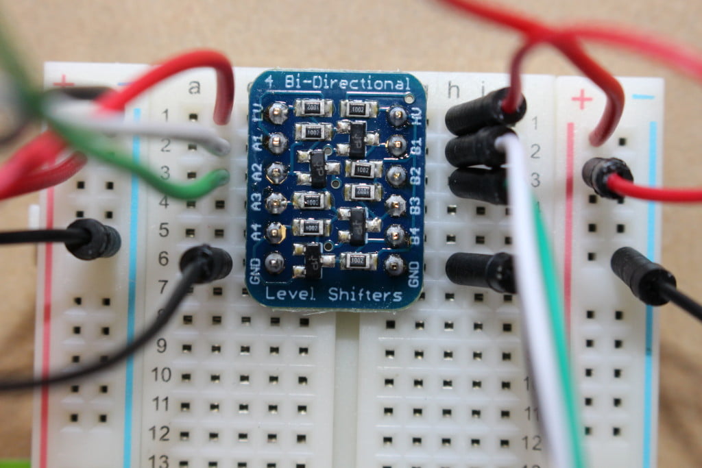
Next, insert the level shifter breakout board into the breakout board. In the video, row 1, column d (1d) corresponds to the LV pin on the level shifter board. This will be referred to as the left side or ‘low voltage side’. The level shifter board should straddle the middle of the breakout board. The middle dividing line of the breakout board indicates that the rows do not tie across to the different sides. For example, row 1 slots a through e are tied together and slots f through j are tied together. The two groups are not connected.
There are two power rails on the breakout board. One power rail will be 1.8V (left side +, low voltage+), the other 3.3V (right side +, high voltage +). Each power rail also has a corresponding ground rail. The ground rails will be common between the two power rails by tying them together.
Insert the GPS breakout board by inserting the pin marked 3.3V into 28h. The GPS will be ‘upside down’, but this will make it easier to wire.
Let’s get started wiring the breadboard. Here’s the wiring:
Level Shifter
GPS
Power
Breadboard to Level Shifter
2 low voltage + to 1 b (1.8V to LV)
5 low voltage – to 6 b (GND to LV GND)
2 high voltage + to 1 h (3.3V to HV)
5 high voltage – to 6 h (GND to HV GND)
Breadboard to GPS
21 high voltage + to 21 j (3.3V to VIN)
22 high voltage – to 22 j (GND to GND)
Tie the ground planes together:
30 low voltage – to 30 high voltage –
Signals
High voltage side, from GPS to Level Shifter
23 j to 2 h (RX to B1)
24 j to 3 h (TX to B2)
Wiring the Jetson to the Breadboard
Power
Jetson to Breadboard
J3A1 Pin 3 to 1 low voltage + (1.8V to breadboard power rail)
J3A1 Pin 2 to 1 low voltage – (Jetson GND to breadboard GND)
J3A1 Pin 16 to 1 high voltage + (Jetson 3.3V to breadboard high voltage)
Signals
J3A2 Pin 68 to 2 b (UART2 TXD Transmit to A1)
J3A2 Pin 65 to 3 b (UART2 RXD Receive to A2)
It should look something like this:

Wiring Note
UARTs are connected to serial devices over two signals, RX (receive) and TX (transmit). The wires are crossed, that is, RX on the UART goes to TX of the device, and TX on the UART goes to RX of the device. The wiring described above does exactly that, the switch occurs at the level shifter.
Off to Part 3, Testing.
Back to Part 1.


