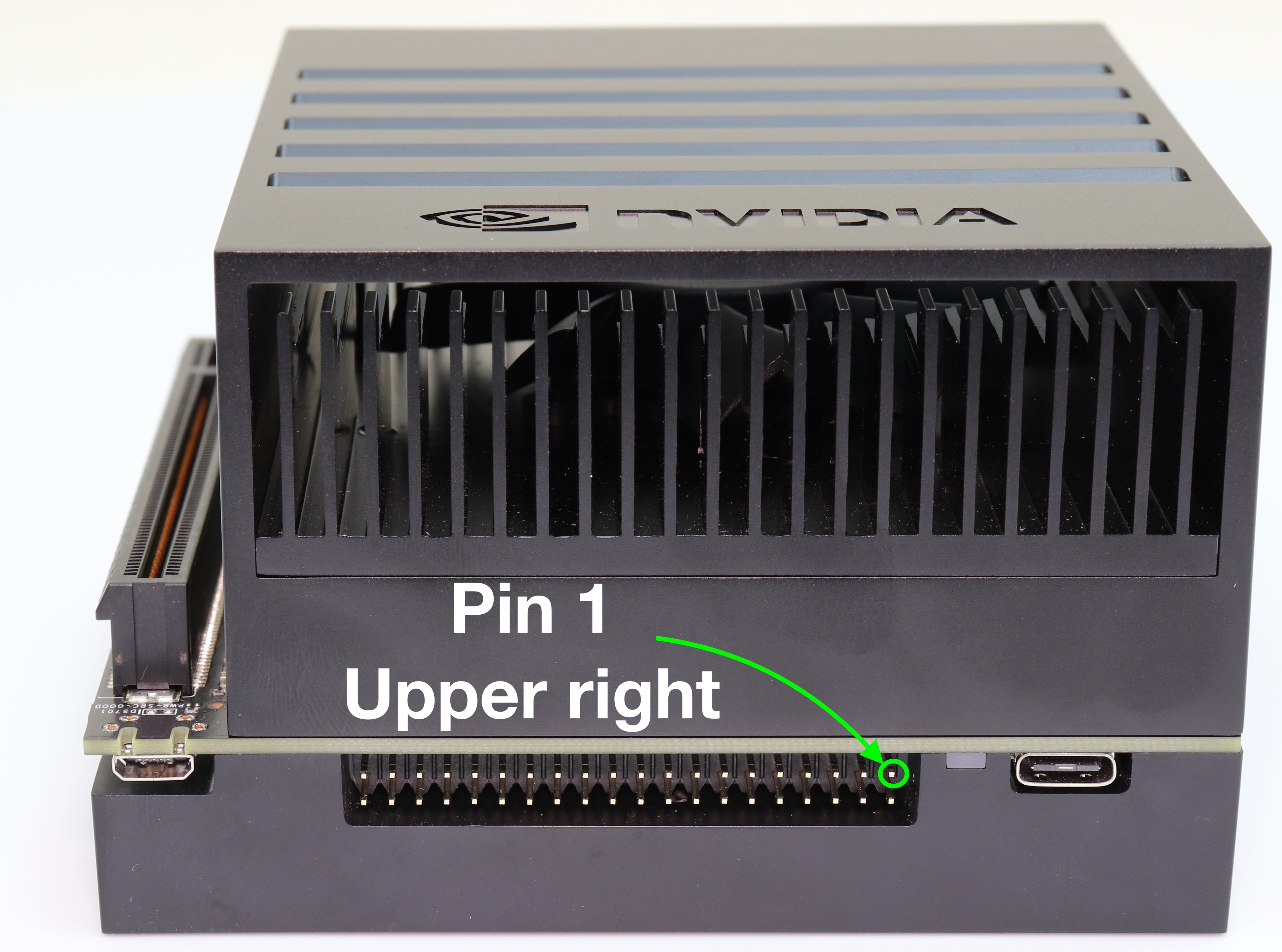
JETSON AGX XAVIER J30 GPIO EXPANSION HEADER PINOUT
Last updated November 7, 2018
| Jetson AGX Xavier Expansion Header | |||||
|---|---|---|---|---|---|
| Sysfs GPIO | Connector Label | Pin | Pin | Connector Label | Sysfs GPIO |
| 3.3 VDC Power, 1A max | 1 | 2 | 5.0 VDC Power, 1A max | ||
| I2C_GP5_DAT General I2C #5 Data 1.8/3.3V, I2C Bus 8 | 3 | 4 | 5.0 VDC Power, 1A max | ||
| I2C_GP5_CLK General I2C #5 Clock 1.8/3.3V, I2C Bus 8 | 5 | 6 | GND | ||
| gpio422 | MCLK05 Audio Master Clock 1.8/3.3V | 7 | 8 | UART1_TX UART #1 Transmit 3.3V | |
| GND | 9 | 10 | UART1_RX UART #1 Receive 3.3V | ||
| gpio428 | UART1_RTS UART #1 Request to Send 1.8/3.3V | 11 | 12 | I2S2_CLK Audio I2S #2 Clock 1.8/3.3V | gpio351 |
| gpio424 | PWM01 Pulse Width Modulation #1 1.8/3.3V | 13 | 14 | GND | |
| gpio393 | GPIO27_PWM2 GPIO/Pulse Width Modulation #2 1.8/3.3V | 15 | 16 | GPIO8_AO_DMIC_IN_DAT Digital Mic Input 3.3V | gpio256 |
| 3.3 VDC Power, 1A max | 17 | 18 | GPIO35_PWM3 GPIO/Pulse Width Modulation #3 1.8/3.3V | gpio344 | |
| gpio493 | SPI1_MOSI SPI #1 Master Out/Slave In 1.8/3.3V | 19 | 20 | GND | |
| gpio492 | SPI1_MISO SPI #1 Master In/Slave Out 1.8/3.3V | 21 | 22 | GPIO17_40HEADER GPIO 1.8/3.3V | gpio417 |
| gpio491 | SPI1_SCLK SPI #1 Shift Clock 1.8/3.3V | 23 | 24 | SPI1_CS0 SPI #1 Chip Select #0 1.8/3.3V | gpio494 |
| GND | 25 | 26 | SPI1_CS1 SPI #1 Chip Select #1 1.8/3.3V | gpio495 | |
| I2C_GP2_DAT General I2C #2 Data 1.8/3.3V, I2C Bus 1 | 27 | 28 | I2C_GP2_CLK General I2C #2 Clock 1.8/3.3V, I2C Bus 1 | ||
| gpio251 | CAN0_DIN CAN #0 Data In 3.3V | 29 | 30 | GND | |
| gpio250 | CAN0_DOUT CAN #0 Data Out 3.3V | 31 | 32 | GPIO9_CAN1_GPIO0_DMIC_CLK Digital Mic Input Clock 3.3V | gpio257 |
| gpio248 | CAN1_DOUT CAN #1 Data Out 3.3V | 33 | 34 | GND | |
| gpio354 | I2S_FS AUDIO I2S #2 Left/Right Clock 1.8/3.3V | 35 | 36 | UART1_CTS UART #1 Clear to Send 1.8/3.3V | gpio429 |
| gpio249 | CAN1_DIN CAN #1 Data In 3.3V | 37 | 38 | I2S_SDIN Audio I2S #2 Data In 1.8/3.3V | gpio353 |
| GND | 39 | 40 | I2S_SDOUT Audio I2S #2 Data Out 1.8/3.3V | gpio352 |
Note: 1.8V/3.3V Selectable by J514

Notes
Here is a spreadsheet which maps the GPIO signals back through the carrier board, to the module, and to the Tegra chip itself:
Default Setup
The initial pinmux should set all of the these pins, except for the power, UART RX TX and two I2C busses, to GPIO at boot. The UART and I2C busses should not be used for GPIO.
Usage designations
The usages described in the above table is the official NVIDIA suggested pin usage for SFIO functionality. A modified device tree or modification to the appropriate registers is required before using as the described function.
Additional Information
Additional information for values in the table and notes are take from Section 3.3 Expansion Header and Table 18. Expansion Header Pin Descriptions in the document “NVIDIA Jetson Xavier Developer Kit Carrier Board Specification” available from the NVIDIA Developer download center.
I2C
Pins 3 and 5 are on I2C bus 8. For detection:
$ sudo i2cdetect -y -r 8
Pins 27 and 28 are on I2C bus 1. For detection:
$ sudo i2cdetect -y -r 1
CAN Bus
- From the Xavier Forum: At present (In case of Xavier) the pinmux which is packaged for Xavier on public releases, configures the CAN I/O pins to have GPIO functionality.
This is to comply with Raspi 40-pin standard.
In this case CAN functionalities are disabled on the pins.To have the pins configured as CAN (SFIO) functionalities, either of these can be followed.
1. There is a separate pinmux configuration to be used in flashing.
Pinmux name: $TEGRA_TOP/ hardware/nvidia/platform/t19x/galen/bct/pinmux/tegra19x-mb1-pinmux-p2888-slvs-0000-a00-p2822-0000-a00.cfg
2. corresponding register values can be overwritten after the system boots.
Reg Val0x0c303000 = 0x0000c400;
0x0c303008 = 0x0000c458;
0x0c303010 = 0x0000c400;
0x0c303018 = 0x0000c458;Any reg read/write tool can be used to overwrite.
However in 2nd case, the register configurations will not be persistent across reboots. - Caution must be taken when using the CAN[1:0]_DIN, CAN[1:0]_DOUT pins (Exp. Conn. pins 37, 29, 33 & 31). These are pulled to 3.3V when system is powered on due to internal 3.3V pull-ups in the SoC enabled by default. If used, they should only be connected to 3.3V tolerant device pins. The voltage rail can be switched by SW after boot to 1.8V, & the internal pull-ups can be disabled, but the initial power-on state of these pins is pulled to 3.3V.
- GPIO Max Drive or Power Pin Current Capability are available in Table 18. Expansion Header Pin Descriptions.
- Pin types and direction are available in Table 18. Expansion Header Pin Descriptions.
- Signal details are available in Table 19. Jetson Xavier Expansion Header Signal Details