JETSON TX2 HEADER PINOUT
This is the Jetson TX2 J21 GPIO Header Layout. Last updated July 18, 2018
The GPIO numbering is different than the Jetson TX1 table.
| Jetson TX2 J21 Header | |||||
|---|---|---|---|---|---|
| Sysfs GPIO | Connector Label | Pin | Pin | Connector Label | Sysfs GPIO |
| 3.3 VDC Power | 1 | 2 | 5.0 VDC Power | ||
| SDA1 General I2C Data 3.3.V, I2C Bus 1 | 3 | 4 | 5.0 VDC Power | ||
| SCL1 General I2C Clock 3.3.V, I2C Bus 1 | 5 | 6 | GND | ||
| gpio396 | GPIO_GCLK Audio Master Clock (1.8/3.3.V) | 7 | 8 | TXD0 UART #0 Transmit | |
| GND | 9 | 10 | RXDO UART #0 Receive | ||
| gpio466 | GPIO_GEN0 UART #0 Request to Send | 11 | 12 | GPIO_GEN1 Audio I2S #0 Clock | gpio392 |
| gpio397 | GPIO_GEN2 Audio Code Interrupt | 13 | 14 | GND | |
| gpio255 | GPIO_GEN3 From GPIO Expander (P17) | 15 | 16 | GPIO_GEN4 Unused | gpio296 |
| 3.3 VDC Power | 17 | 18 | GPIO_GEN5 Modem Wake AP GPIO | gpio481 | |
| gpio429 | SPI_MOSI SPI #1 Master Out/Slave In | 19 | 20 | GND | |
| gpio428 | SPI1_MISO SPI #1 Master In/Slave Out | 21 | 22 | GPIO_GEN6 From GPIO Epander (P16) | gpio254 |
| gpio427 | SPI_SCLK SPI #1 Shift Clock | 23 | 24 | SPI_CE0_N SPI Chip Select #0 | gpio430 |
| GND | 25 | 26 | SPI_CE1_N SPI #1 Chip Select #1 | ||
| ID_SD General I2C #1 Data (3.3V), I2C Bus 0 | 27 | 28 | ID_SC General I2C #1 Clock (3.3V), I2C Bus 0 | ||
| gpio398 | GPIO5 Audio Reset (1.8/3.3V) | 29 | 30 | GND | |
| gpio298 | GPIO6 Motion Interrupt (3.3V) | 31 | 32 | GPIO12 Unused | gpio297 |
| gpio389 | GPIO13 AP Wake Bt GPIO | 33 | 34 | GND | |
| gpio395 | GPIO19 AUDIO I2S #0 Left/Right Clock | 35 | 36 | GPIO16 UART #0 Clear to Send | gpio467 |
| gpio388 | GPIO26 (3.3V) | 37 | 38 | GPIO20 Audio I2S #0 Data in | gpio394 |
| GND | 39 | 40 | GPIO21 Audio I2S #0 Data in | gpio393 |
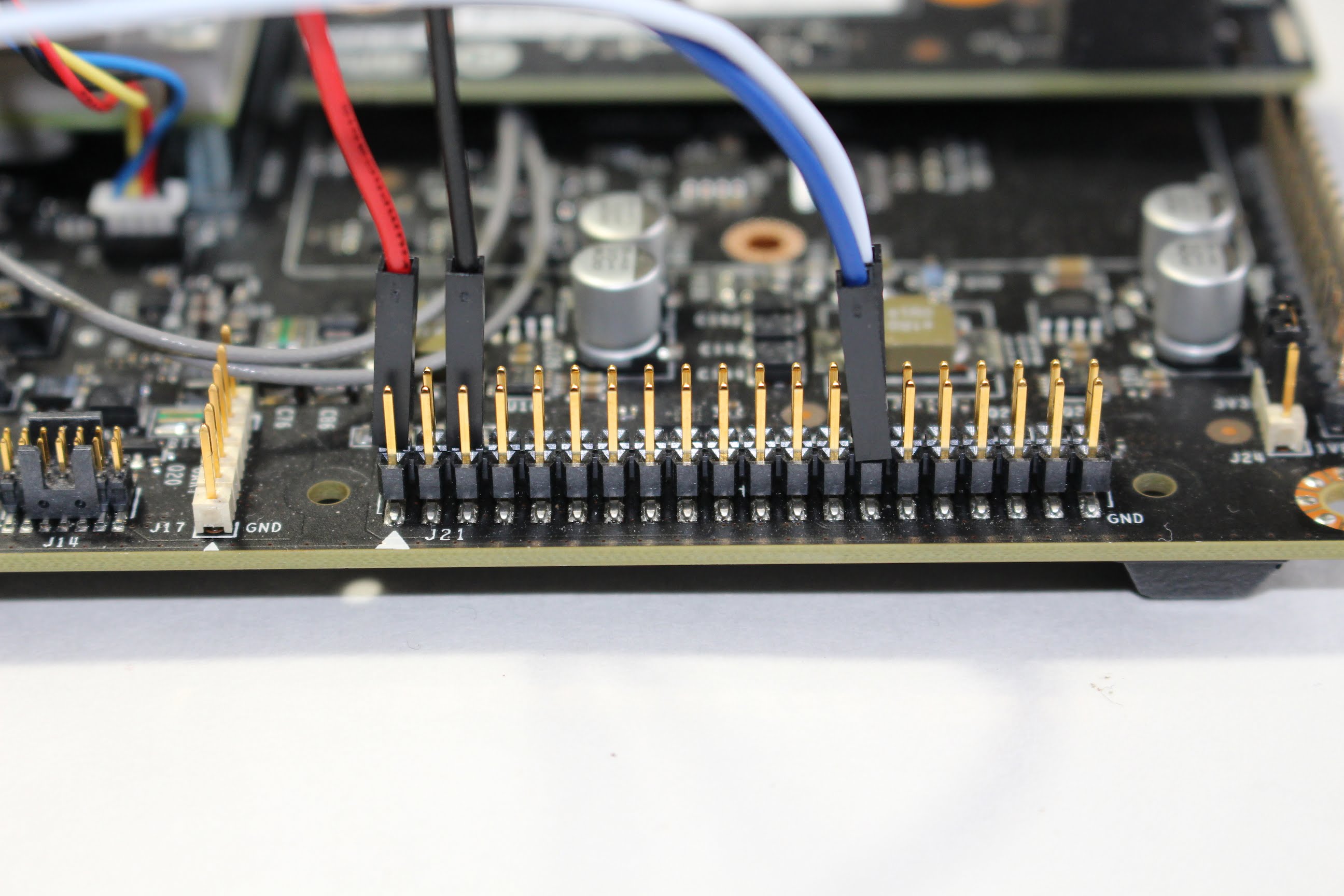
Note: The arrow on the circuit board points to pin 1. Pin 2 is behind pin 1 in the picture.
The I2C bus numbers are swapped in comparison to the Jetson TX1.
I2C Bus 0 address 0x0040-0x0043 are the INA3221x power monitors.
Here is a spreadsheet which maps the J21 signals back through the carrier board, to the module, and to the Tegra chip itself: